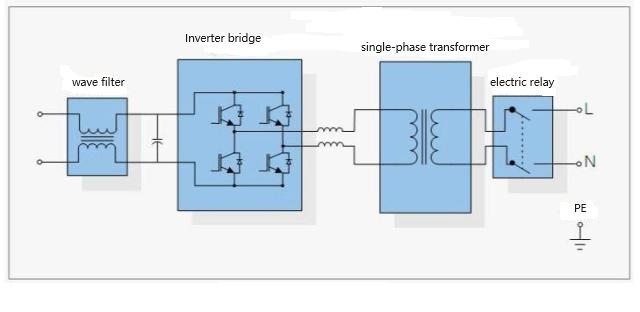
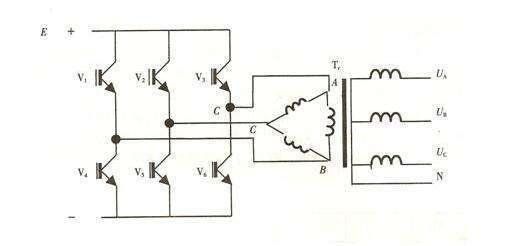
Input interface section:
There are three signals in the input section: 12V DC input VIN, working enable voltage ENB, and panel current control signal DIM. VIN is provided by the Adapter, and ENB voltage is provided by the MCU on the motherboard, with a value of 0 or 3V. When ENB=0, the inverter does not work, while when ENB=3V, the inverter is in normal working condition; The DIM voltage is provided by the motherboard, with a range of 0-5V. Different DIM values are fed back to the feedback terminal of the PWM controller, and the current provided by the inverter to the load will also be different. The smaller the DIM value, the larger the
current output by the inverter.

Voltage starting circuit:
When ENB is at high level, output high voltage to light up the backlight tubes of the panel.
PWM controller: It consists of the following functions: internal reference voltage, error amplifier, oscillator and PWM, overvoltage protection, undervoltage protection, short circuit protection, and output transistor.
DC conversion:
A voltage conversion circuit is composed of MOS switching transistors and energy storage inductors. The input pulse is amplified by a push-pull amplifier to drive the MOS transistor to perform switching actions, so that the DC voltage charges and discharges the inductor, and the other end of the inductor can obtain AC voltage.
LC oscillation and output circuit:
Ensure the required voltage of 1600V for lamp start-up and reduce the voltage to 800V after lamp start-up.
Output voltage feedback:
When the load is working, the feedback sampling voltage plays a role in stabilizing the Inventor voltage output.
You can actually imagine it. What electronic components require positive and negative poles, resistors, and inductors are generally not needed. The possibility of a diode breaking down is usually due to breakdown, as long as the voltage is normal, there is generally no problem. For a transistor, it will not conduct. If the positive and negative connections of the voltage regulator are reversed, it will be damaged, but usually some circuits are protected by the unidirectional conduction of diodes. In capacitors, there is a distinction between positive and negative, which is electrolytic capacitors. If the positive and negative
connections are reversed severely, the casing will explode.

The main component is the diode. Switching tube oscillating transformer. Sampling. Widening tube. There is also the principle of parametric switching circuits such as oscillating circuits, resistors, capacitors, etc. The selection of the main power components for inverters is crucial. Currently, the most commonly used power components include Darlington Power Transistors (BJTs), Power Field Effect Transistors (MOSFETs), Insulated Gate Transistors (IGBTs), and Turn Off Thyristors (GTOs). MOSFETs are more commonly used in small capacity and low voltage systems because they have lower on state voltage drop and higher switching frequency. IGBT modules are generally used in high voltage and large capacity systems because their on state resistance increases with increasing voltage. IGBTs have a significant advantage in medium capacity systems, while GTOs are generally used as power components in ultra large capacity (100KVA and above) systems.
Large components: Field effect transistors or IGBTs, transformers, capacitors, diodes, comparators, and main controllers such as 3525. AC-DC-AC inverter and rectification filtering.
The power level and accuracy are related to the complexity of the circuit.
IGBT (Insulated Gate Bipolar Transistor), as a new type of power semiconductor field controlled self turn off device, combines the high-speed performance of power MOSFET with the low resistance of bipolar devices. It has the characteristics of high input impedance, low voltage control power consumption, simple control circuit, high voltage resistance, and large current tolerance, and has been widely used in various power conversions. At the same time, major semiconductor manufacturers are constantly developing IGBT technologies with high withstand voltage, high current, high speed, low saturation voltage drop, high reliability, and low cost, mainly using manufacturing processes below 1um, and making some new progress in research and development.
1. Working principle of fully controlled inverter
For the commonly used single-phase output full bridge inverter main circuit, the AC components use IGBT transistors Q11, Q12, Q13, and Q14. The conduction or cutoff of the IGBT transistors is controlled by PWM pulse width modulation.
When the inverter circuit is connected to a DC power supply, Q11 and Q14 are turned on first, and Q1 and Q13 are turned off. The current is output from the positive pole of the DC power supply, passes through Q11, L or the primary coil of the transformer shown in Figure 1-2, and returns to the negative pole of the power supply at Q14. After Q11 and Q14 are turned off, Q12 and Q13 are turned on, and the current flows from the positive pole of the power supply through Q13 and the inductor of the transformer primary coil 2-1 to Q12 and returns to the negative pole of the power supply. At this point, positive and negative alternating square waves have been formed on the primary coil of the transformer. Using high-frequency PWM control, two pairs of IGBT tubes alternate and repeat, generating AC voltage on the transformer. Due to the action of the LC AC filter, a sine wave AC voltage is formed at the output terminal。
When Q11 and Q14 are turned off, in order to release stored energy, diodes D11 and D12 are connected in parallel at the IGBT to return the energy to the DC power supply.
tags :
scan to wechat:everexceed
